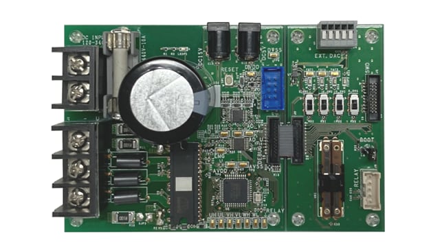
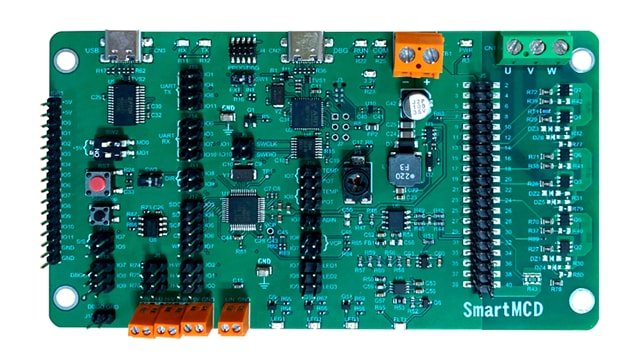
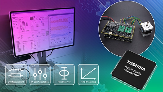
On July 1st, Toshiba Corporation's Semiconductor Company and Storage Products Company consolidated to form Semiconductor & Storage Products Company.This page describes reliability information of semiconductor products.
Failure Mechanisms
[As of April, 2011]
Si-SiO2 Interface
Semiconductor chips based on the surface phenomenon exhibit characteristics which vary greatly depending on the state of the Si-SiO2 interface. There are many complex failure mechanisms related to this phenomenon.
Failure mechanisms related to the Si-SiO2 interface include those induced by the substrate and those induced by the gate oxide film or surface protective film. The latter are described in the sections entitled "Gate Oxide Film" and "Passivation." The former is described below.
Degradation Due to Hot CarriersNote 1
When voltage is applied to the drain of a miniaturized N-channel MOS transistor, a large electrical field is generated in the drain region as shown in Figure 1. As carriers flow into this region, they gain energy from the electrical field and become hot carriers. Some of them are scattered by phonons and others lose energy due to impact ionization.
Hot carriers with enough energy to surmount the Si-SiO2 electrical potential barrier are injected into the gate oxide film. This phenomenon, which accelerates with voltage, changes the MOS transistor threshold (Vth) and the mutual conductance (Gm).
There are four known gate oxide film carrier injection/capture mechanisms, based on MOS transistor bias conditions: channel hot electrons (CHE), drain avalanche hot carrier injection (DAHC), two-port hot electrons and substrate hot electrons.Note 2
To avoid the effects of hot carriers, countermeasures are taken, such as reducing the circuit’s internal operating voltage or forming a gate oxide film which does not readily trap injected hot carriers. Various measures are taken with the transistor structure, especially for devices with a gate length of 2 µm or less. One such measure is a lightly doped drain (LDD) transistor, as shown in Figure 4.Note 3
This structure exhibits a smaller electrical field around the drain and thus has fewer hot carriers.
Degradation of device characteristics due to hot carriers also occurs in bipolar transistors. This is a well-known phenomenon in which hFE degradation occurs when a reverse bias is applied across the emitter and base. With the advanced shallow junction devices of recent years, there is a tendency towards increased reverse leakage current between the emitter and base, causing device characteristic degradation to readily occur as a result of the hot carrier effect.
Figure 3 shows an example of high-frequency characteristic ƒt degradation caused by reverse emitter-base bias. This is because the base current increases due to an increased number of recombination centers at the Si-SiO2 interface caused by hot carrier injection during reverse biasing.
Many of the semiconductor device failure modes exhibit higher degradation at higher temperatures. In contrast, hot carriers are characterized by higher degradation at lower temperatures.
![This is [Figure 1 Hot Carrier Injection Model]. This is [Figure 1 Hot Carrier Injection Model].](/eng/product/reliability/device/failure/__icsFiles/artimage/2009/09/28/ec_relia05_2/E_02-020_z03-03_300.gif)
Figure 1 Hot Carrier Injection Model
![This is [Figure 2 Lightly Doped Drain (LDD) Structure Transistor]. This is [Figure 2 Lightly Doped Drain (LDD) Structure Transistor].](/eng/product/reliability/device/failure/__icsFiles/artimage/2009/09/28/ec_relia05_2/E_02-020_z03-04_300.gif)
Figure 2 Lightly Doped Drain (LDD) Structure Transistor
![This is [Figure 3 Degradation of RF Characteristics (ƒ<sub>t</sub>) Due to Reverse Emitter Bias]. This is [Figure 3 Degradation of RF Characteristics (ƒ<sub>t</sub>) Due to Reverse Emitter Bias].](/eng/product/reliability/device/failure/__icsFiles/artimage/2009/09/28/ec_relia05_2/E_02-020_z03-05_300.gif)
Figure 3 Degradation of RF Characteristics (ƒt) Due to Reverse Emitter Bias
Characteristic Degradation Due to Voltage StressNote 4
When a bias is applied under high temperature conditions to the MOS transistor gate or drain, the fixed charge and interface state in the gate oxide film reportedly increases, causing Vth shift and a reduction in driving current which in turn causes characteristic degradation (BTI: Bias Temperature Instability). In recent years, negative bias temperature instability (NBTI) has particularly become problematic when a negative bias is applied under high temperature conditions to 3 µm or less thin film PMOS transistor gate. Possible NBTI degradation mechanisms include the interface state and fixed positive charge generated when hydrogen is dissociated from the Si-H bond of the interface. Another possible mechanism is a model based on the positive hole trap produced by the impact ionization collision on the Si surface of electrons tunneled into the substrate from the gate electrode. The dependency on processing conditions has also been revealed in recent years. Reports indicate that elements such as nitrogen, hydrogen and water which form a charge trap in gate oxide film affect NBTI degradation. Process development therefore requires optimization of the N and H concentrations in the gate oxide film as well as the interface state.
Noise Charge Due to Impact IonizationNote 5
In the other failure mechanism caused by impact ionization, positive holes (in an N-channel device) from the electron-hole pairs generated by previous impact ionization are accelerated towards the substrate, causing secondary impact ionization. These pairs reach the immediately adjacent memory cells and CCD cells as noise charge, filling storage capacitors with the charge and inverting their memory states. This failure mechanism should not be neglected, as scaling levels will become even greater in the future.
Soft ErrorsNote 6
With increasing device miniaturization, α-particles radiated from minute amounts of radioactive elements (uranium and thorium) contained in packaging and wiring material have become problematic. When an α-particle impinges on the PN junction area inside a device, an electron-hole pair is generated in accordance with the range. The small number of carriers produced inverts the device information inside the DRAM or SRAM memory cell. This phenomenon is referred to as a "soft error." Soft errors are broadly classified into memory cell mode errors and bit line mode errors.
A memory cell mode error occurs when an α-particle impinges on a memory cell area. The electrons generated by the impinging α-particle and the resultant energy attenuation subsequently flow into the memory cell area and corrupt the data.
In a bit line mode error, the electron-hole pair generated by the α-particle produces an electrical current, affecting the bit line information voltage or the reference voltage.
Soft Error Rate is therefore dependent on cycle time while others are not. Under normal conditions, when data is read, data from the cell is transmitted on the bit line, generating a small charge. This small charge is then compared with the reference charge and amplified by a sense amplifier so that the data can be read. When the cycle time increases, the chance for reference charge and data comparisons also increases. Thus, bit line mode errors are dependent on cycle time while memory cell mode errors are not.
In order to reduce the soft error effects caused by α-particles, measures such as applying high-purity material (such as low α-particle resin) are taken.
In recent years, soft errors have been reported to occur due to cosmic rays and, particularly, neutrons.
When cosmic rays (protons and charged particles of He, etc.) enter the atmosphere and collide with atmospheric elements, secondary particles are produced. The neutrons that are not charged reach the earth’s surface, attenuating only at nuclear collision in the atmosphere.
The neutrons in cosmic rays are classified into high-energy neutrons of 10 to a few 100 MeV, and low energy neutrons that reach a thermal equilibrium at the earth’s surface.
When high-energy neutrons collide with the Si nucleus of a device, the generated charged ions induce a large load, resulting in a soft error. The Li and α-particles produced from a capture reaction with low energy neutrons (thermal neutrons) and 10B are known to cause soft errors. These particles especially have a great effect on devices that employ boron phosphorus silicon glass (BPSG), which contain a lot of 10B.
Neutron-induced soft errors depend on the operating environment of the device, such as the geographical environment (latitude, longitude, altitude, etc.) and radiation shielding environment (indoor/outdoor), and the radiation environment on the ground depends on factors such as solar activity.
![This is [Figure 4 Soft Error Mechanisms]. This is [Figure 4 Soft Error Mechanisms].](/eng/product/reliability/device/failure/__icsFiles/artimage/2009/09/28/ec_relia05_2/E_02-022_z03-06_450.gif)
Figure 4 Soft Error Mechanisms
Note 1: Bibliography. Bruce Euzent; "Hot Electron Injection Efficiency in IGFET Structures," 15th Annual Proc. Re1. Phys., (1977), p. 1
Note 2: Bibliography. Taniguchi; "Silicon Thermal Oxide Film and its Interface," Realize Advanced Technology Limited, (1991), p. 296
Note 3: Bibliography. Iizuka, Sakurai, Kakumu; "Taking Advantage of Circuit Technology to Protect 1 µm MOS LSI from Hot Carrier," Nikkei Microdevice, 1985 summer special issue
Note 4: Bibliography. M. Makabe; IEEE Trans. IRPS Proc., (2000), p. 205
Note 5: Bibliography. Furuyama, Kayama; "Malfunction of Dynamic Memory due to Impact Ionization," Nikkei Electronics, March 3 (1980), p. 120
Note 6: Bibliography. T. C. May and M. H. Woods; “A New Physical Mechanism for Soft Errors in Dynamic Memories,” 16th Annual Proc, Rel., (1987), p. 33
On July 1st, Toshiba Corporation's Semiconductor Company and Storage Products Company consolidated to form Semiconductor & Storage Products Company.This page describes reliability information of semiconductor products.


